Quantum computing has long promised breakthroughs in chemistry, logistics, finance, and climate modeling, but the hardware has struggled to scale beyond fragile lab prototypes. A new generation of tiny, highly specialized chips is starting to change that trajectory, shrinking critical components to microchip size and attacking the field’s biggest bottleneck: error-prone, unwieldy qubits. If these designs deliver, the leap from experimental machines to practical quantum accelerators could arrive faster than many expected.
Instead of chasing ever larger headline qubit counts, researchers are quietly rethinking the building blocks themselves, from superconducting circuits to photonic networks and exotic quasiparticles. I see a clear pattern emerging across corporate labs and universities: the most interesting progress is happening where engineers compress control, error correction, and interconnects into compact, manufacturable devices that look less like science projects and more like the early integrated circuits of classical computing.
The tiny device that reframes “scale”
The clearest symbol of this shift is a new microchip-sized device that researchers describe as a “Tiny Device Built for Real-World Scale.” Instead of treating the quantum processor as a single monolithic machine, this approach packs the essential quantum control and interconnect functions into a chip that can be tiled, networked, and mass produced, much like classical processors. The team behind it argues that this architecture could eventually support systems far more powerful than anything possible today, not by chasing a single giant quantum die but by stitching together many small, robust units.
In practical terms, that means rethinking how qubits are created, routed, and stabilized so that each miniature module can plug into a larger fabric without collapsing under noise. The work, highlighted under the banner Tiny Device Built for Real, World Scale, frames scale as a systems problem rather than a single-chip race. I read this as a deliberate pivot away from brute-force qubit counts and toward modularity, where reliability and manufacturability matter as much as raw quantum capacity.
From lab curiosities to a “transistor moment”
What makes this new class of chips so consequential is not just their size, but the way they echo the integrated circuit revolution that transformed classical electronics. One recent analysis describes how a compact photonic device could, in the long run, trigger a kind of “transistor revolution” for optics, doing for quantum hardware what the integrated circuit did for early computers. Instead of sprawling optical benches and bespoke cryogenic setups, the vision is to integrate sources, detectors, and routing elements on a single piece of silicon that can be replicated at scale.
That argument is laid out in detail in a discussion of how a tiny chip breakthrough could supercharge quantum computers by making it practical to control very large numbers of qubits. I see the parallel to the 1950s and 1960s, when the move from discrete transistors to integrated circuits suddenly made it feasible to pack thousands, then millions, of components onto a single die. If quantum hardware can follow a similar path, the field’s current reliance on handcrafted, one-off machines will give way to standardized modules that can be slotted into data centers and specialized appliances.
Google’s Willow and the race to tame errors
Nowhere is the shift toward compact, scalable design clearer than in Google’s new quantum chip, Willow. The company describes Willow as a state-of-the-art processor that significantly reduces errors as it scales, a crucial step toward making quantum computation reliable enough for real workloads. Rather than simply adding more qubits, Willow focuses on improving the quality of those qubits and the stability of their interactions, which is the only way to make error correction codes practical.
In its own technical overview, Google frames Willow as a platform for tackling problems in medicine, energy, and AI once the error rates fall below key thresholds. A separate analysis of Willow’s performance argues that the chip can, in specific benchmark tasks, outpace the world’s fastest supercomputers by astronomical margins, compressing computations that would take longer than the age of the universe on classical hardware into feasible runtimes. I read those claims as early, highly specialized demonstrations rather than general-purpose speedups, but they underscore how much leverage a well-designed quantum chip can have once error rates are under control.
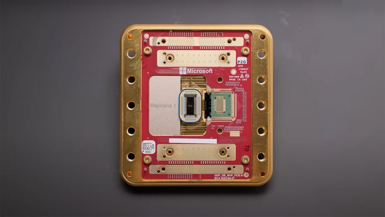
Majorana 1 and the quest for topological stability
While Willow refines superconducting qubits, Microsoft is betting on a more radical path with its Majorana 1 hardware. The company has introduced a device built around so-called Majorana modes, exotic quasiparticles that could, in theory, encode information in a way that is inherently protected from certain types of noise. The architecture used to develop the Majorana 1 prototype is presented as a new route toward fault-tolerant quantum computing, one that aims to solve real-world scientific and societal problems by reducing the overhead of error correction.
Microsoft’s own description of Majorana 1 highlights how the device is built on an architecture that could, if the physics holds up, support more stable logical qubits than conventional designs. A complementary technical summary notes that Majorana 1 is a hardware device developed by Microsoft for use in quantum computing and that it is the first device publicly described as realizing this kind of topological qubit. I see this as a high-risk, high-reward bet: if topological protection works as advertised, it could slash the number of physical qubits needed per logical qubit, making large-scale machines far more compact.
Princeton’s blueprint for scalable superconducting chips
Academic labs are also rethinking chip architecture with scale in mind, and Princeton’s new quantum chip is a prime example. The device is explicitly described as “built for scale,” and it comes from a team that includes Andrew Houck, who co-invented the transmon superconducting qubit in 2007. That pedigree matters, because the transmon design underpins many of today’s leading superconducting platforms, and any new architecture from the same lineage carries significant weight.
The Princeton team’s work on a quantum chip built for scale focuses on how to route control lines, manage crosstalk, and integrate large numbers of qubits without overwhelming the cryogenic environment. By emphasizing layout and connectivity as much as the qubits themselves, the design anticipates the engineering headaches that will come with thousands of superconducting elements on a single chip. I read this as a quiet but important shift: the frontier is no longer just about inventing a better qubit, but about making sure those qubits can coexist on a dense, manufacturable die.
Photonic shortcuts and China’s 1000x ambition
Superconducting and topological approaches are not the only routes to compact quantum hardware. Photonics, which uses individual photons as information carriers, offers a way to operate at or near room temperature and to leverage existing semiconductor fabrication techniques. A recent report on a Chinese effort describes a quantum photonic chip that aims to be 1000 times more capable than current designs, positioning it as a potential leap in the global race toward optical quantum computing.
The discussion of how China develops a quantum photonic chip 1000X more powerful also notes that this push is happening in parallel with investments from companies like Nvidia in optical interconnects and photonic accelerators. I see this convergence as significant: if photonic quantum chips can be manufactured on the same lines as advanced optical networking hardware, the path from prototype to deployment could be shorter than many expect. The challenge, as always, will be integrating sources, detectors, and error mitigation on a chip small enough and cheap enough to replicate at scale.
Classical miniaturization sets the pace
One reason the quantum world is suddenly obsessed with tiny chips is that classical semiconductor manufacturing keeps shrinking the baseline. MediaTek, for example, is preparing to roll out what it describes as the world’s smallest chip from September 2025, a milestone that underscores how far advanced lithography and packaging have come. When a mainstream mobile and IoT supplier can mass produce such devices, it raises expectations for what quantum hardware should eventually look like.
The company’s leadership, including CEO Rick Tsai, frames this push as part of a broader strategy to dominate ultra-compact, low-power silicon. I interpret that as a signal to quantum engineers: if your design cannot, in principle, be mapped onto something that fits within the constraints of modern fabs and packaging houses, it will struggle to compete. The bar for “tiny” is being set by consumer electronics, and quantum devices will eventually have to meet it.
Industry leaders converge on chip-centric roadmaps
Across the sector, major players are aligning around chip-centric strategies that treat quantum processors as modular accelerators rather than standalone curiosities. A recent overview by Marin Ivezic, who is CEO of Applied Quantum and a Former CISO and Big 4 Partner, surveys five new chips that are pushing the boundaries of quantum computing and highlights how each one tackles a different piece of the scalability puzzle. Some focus on error correction, others on connectivity or integration with classical control electronics, but all share a commitment to compact, manufacturable designs.
In that analysis of five new chips, the common thread is that quantum hardware is starting to look less like bespoke physics experiments and more like products with clear roadmaps. I see this as a maturation point for the industry: when CEOs and security leaders talk about quantum chips in the same breath as traditional accelerators, it signals that the technology is moving into the realm of strategic planning rather than speculative research alone.
Headline-grabbing speedups and public expectations
As these chips improve, public expectations are being shaped by dramatic performance claims. Google, for instance, has unveiled a quantum computing chip that it describes as “mind-boggling,” asserting that the device can complete certain calculations in minutes that would take classical supercomputers thousands of years and cost billions of dollars. Those demonstrations are carefully chosen benchmarks, but they serve a purpose: they show that even relatively small quantum processors can outperform the largest classical machines on specific tasks.
The report on how Google unveils this chip emphasizes that the feat is not yet a general-purpose advantage, but it does validate the underlying physics and control systems. I read these headline-grabbing results as double-edged: they attract investment and talent, but they can also create unrealistic expectations about how quickly quantum machines will transform everyday computing. The real story, in my view, lies in the quieter engineering work that makes such demonstrations repeatable and eventually useful for real-world workloads.
How a single tiny chip can shift the roadmap
When I look across these developments, from Willow and Majorana 1 to Princeton’s scalable design and China’s photonic ambitions, the throughline is clear: the future of quantum computing will be decided at the chip level. A single tiny device that integrates control, error mitigation, and connectivity in a manufacturable form can unlock architectures that scale by replication rather than by heroic one-off engineering. That is why a microchip-sized quantum module, even with modest qubit counts, can have an outsized impact on the field’s trajectory.
Broader coverage of quantum computers highlights how stories about a “Tiny Chip Could Change the Future of Quantum Computing” are capturing attention alongside more traditional reports on algorithmic advances. I see that as a healthy rebalancing: for years, the conversation has been dominated by abstract promises and distant applications. Now, the focus is shifting to concrete hardware milestones, where a new chip design is judged not just by its novelty, but by whether it can be manufactured, networked, and maintained in the messy reality of data centers and laboratories.
The stakes: from niche experiments to everyday infrastructure
All of this points to a near future in which quantum processors are no longer rare, room-filling machines, but compact accelerators that sit alongside GPUs and TPUs in specialized racks. The tiny chips emerging today are prototypes of that world, where modular quantum units can be swapped, upgraded, and scaled out as workloads demand. If the “transistor revolution” analogy holds, the most important breakthroughs may not be the flashiest demonstrations, but the quiet standardization of interfaces, packaging, and control protocols that let these devices plug into existing infrastructure.
At the same time, the field remains in flux, with multiple architectures competing and no guarantee that any single approach will dominate. The fact that efforts range from This Tiny Chip Could Change the Future of Quantum Computing narratives to ambitious topological and photonic roadmaps shows both the promise and the uncertainty. I come away convinced that the decisive factor will be less about any single physics breakthrough and more about which designs can be shrunk, replicated, and trusted enough to become part of everyday digital infrastructure.
More from MorningOverview