Artificial intelligence has raced ahead so quickly that its biggest constraint is no longer clever algorithms but the plumbing that feeds them data. A new generation of 3D chips, built by stacking logic and memory directly on top of each other, is now emerging as a direct assault on that bottleneck, promising order-of-magnitude speed and efficiency gains for the most data-hungry models. If these designs scale, the shift from flat silicon to vertical computing could matter as much for AI as the move from CPUs to GPUs.
Instead of shuttling information back and forth across circuit boards, these devices keep data and compute in the same dense vertical stack, slashing the distance bits have to travel and the energy burned along the way. Early prototypes already report 4× performance improvements over comparable 2D chips and hint at even larger energy savings, suggesting that the long-feared “memory wall” holding back AI may finally be starting to crack.
The memory wall that AI keeps slamming into
Modern AI workloads are dominated by moving data, not just crunching it. Training a large language model or running real-time perception in a self-driving car means constantly pulling weights and activations from memory into compute units, then writing results back out again. Even as processors have become faster and more parallel, the bandwidth and latency of traditional memory systems have not kept pace, creating what chip designers call the memory wall, a point where performance is limited less by arithmetic and more by how quickly data can be fetched.
In conventional 2D architectures, memory chips sit off to the side of processors, linked by relatively long electrical connections that waste energy and time every time a bit moves. Reporting on a new 3D chip design describes this as one of AI’s biggest data bottlenecks, noting that the architecture is explicitly tuned to attack the memory wall by enabling significantly faster data movement between compute and storage elements in the same stack, rather than across a board-level bus, a shift that directly targets the core inefficiency in today’s accelerators memory wall.
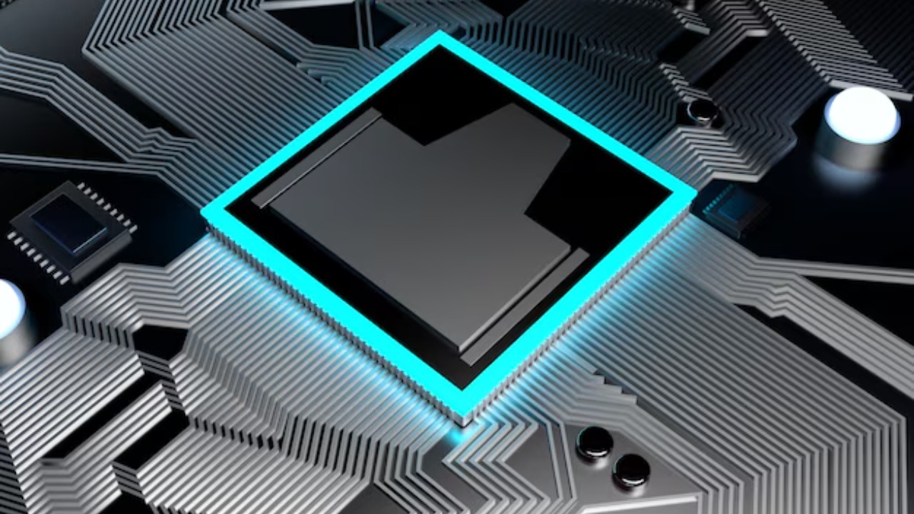
What makes this 3D chip fundamentally different
The new 3D chip does not just stack existing components the way high bandwidth memory does on a GPU package, it integrates memory and logic in a single monolithic structure so that compute layers and storage layers are fabricated sequentially on the same wafer. Researchers describe a design where memory and computing elements are arranged vertically, with dense interconnects running up and down the stack, which allows data to move in three dimensions instead of being confined to a flat plane. That geometry is what lets the device dramatically increase bandwidth while cutting the distance each signal has to travel.
According to Dec Researchers, the prototype 3D chip they built uses this vertical integration to reduce data movement energy and latency compared with conventional flat architectures, and they emphasize that the process is intended to be compatible with real-world production rather than a lab-only curiosity, a point underscored by their claim that the technology is ready for scaling into practical systems 3D computer chip.
Inside Stanford’s monolithic 3D breakthrough
One of the most striking demonstrations of this approach comes from a Dec project at Stanford, where a team built what they describe as a Monolithic 3D AI chip that hits 4× Gains in performance and Points toward a major energy breakout. The key is sequential manufacturing, a process in which multiple layers of devices are fabricated one after another on the same substrate, allowing thousands of vertical connections between logic and memory cells. Instead of routing signals across millimeters of metal traces, the chip can hop data up or down through microscopic vias that are only micrometers apart.
Reporting on the Stanford work notes that this sequential manufacturing enables thousands of vertical interconnects per square millimeter, which in turn allows the designers to replace long electrical links with light and other advanced signaling techniques, a combination that helps explain how the Monolithic device can deliver 4× Gains in AI workloads while also pointing to much larger energy efficiency improvements as the technology matures Monolithic 3D AI chip.
The first truly 3D chip from a US foundry
What makes this wave of research especially significant is that it is not confined to university clean rooms, it is already reaching commercial fabrication lines. A Stanford-led team reports building the first truly 3D chip at a US foundry, integrating carbon nanotube transistors and RAM on a single die in a way that future devices can scale. By putting RAM directly above and below logic layers, the design eliminates the need for separate memory chips and the package-level wiring that connects them, which is exactly where much of today’s AI energy budget is spent.
The group says this device, produced at a domestic facility, delivers 4× performance gains compared with comparable 2D chips, and they highlight that the combination of carbon nanotube transistors with dense RAM in one vertically integrated stack is intended as a template for future AI accelerators that can keep scaling even as traditional silicon approaches its limits, a claim that underscores how central 3D integration has become to the roadmap for advanced computing first truly 3D chip.
SkyWater and the leap from lab demo to factory line
For any chip technology, the real test is whether it can survive the brutal economics and process constraints of a commercial fab. That is why the collaboration between Stanford and SkyWater matters so much: Dec reports describe how a small group of engineers built what they call the world’s first Monolithic 3D chip that runs AI workloads inside a commercial US semiconductor facility, rather than in a bespoke research line. Producing a vertically integrated AI device in a standard foundry environment suggests that the techniques behind these stacks can be slotted into existing manufacturing flows with realistic yields.
SkyWater positions itself as a US-based semiconductor manufacturer focused on advanced technologies, and the fact that this Monolithic 3D AI chip was realized in its production environment signals that 3D integration is moving from theory to practice in the domestic supply chain, a shift that could reshape how designers think about co-locating memory and compute in future accelerators SkyWater Technology. In the context of US industrial policy and the push for more onshore chip capacity, having a commercial foundry capable of fabricating such dense vertical stacks is as strategically important as the performance numbers themselves.
Prototype performance: early numbers and what they mean
Performance claims for new chip architectures are often optimistic, but the early hardware tests for these 3D AI devices are already notable. Dec Early evaluations of one prototype show that it outperforms comparable 2D chips on AI workloads, not just in raw throughput but in energy per operation, which is critical for data centers and edge devices alike. Because the memory and compute elements are stacked, the chip can keep more data on-die and avoid the constant off-chip traffic that drags down today’s accelerators, leading to both speed and efficiency gains.
The same reporting emphasizes that the prototype’s performance and potential are already beyond what conventional flat architectures can realistically reach, given the physical limits on how wide and fast off-chip memory interfaces can be driven without burning excessive power, and it frames the 3D design as a way to sidestep those constraints by changing the geometry of the system rather than just pushing clock speeds higher prototype performance.
Order-of-magnitude speed gains and dense vertical scaling
Beyond the 4× improvements reported in some experiments, other teams are already talking about order-of-magnitude gains. Dec coverage of US engineers working on a 3D AI chip describes devices that offer order-of-magnitude speed gains and accelerate AI by exploiting the same principle of stacking compute and memory in a dense vertical structure. By shortening the distance between logic and storage and multiplying the number of parallel connections, these chips can feed matrix multipliers and other AI primitives far more efficiently than traditional boards that rely on external DRAM.
They also stress that this is not just about raw speed but about opening a new era of chip production, one where 3D integration becomes a standard tool for architects who need to keep scaling performance without relying solely on smaller transistors, a path that is becoming harder as conventional scaling slows order-of-magnitude speed gains. In parallel, Dec reporting on another dense 3D chip for AI processing notes that They designed the device so that it can be built vertically as well as horizontally, with each layer fabricated to support both compute and memory, a choice that underscores how central density and stacking have become to the AI hardware roadmap dense 3D chip.
Energy, bandwidth, and why interconnects are the real story
When I look at these designs, the most important shift is not just the extra compute packed into a given footprint, it is the way they attack interconnect length and bandwidth density, the quiet killers of AI efficiency. Dec analysis of one 3D chip to accelerate AI highlights that by shortening interconnect lengths and increasing bandwidth density, the architecture reduces the energy required to move data between memory and logic, which is often the dominant term in the power budget for large models. In other words, the chip is not just faster because it has more units, it is faster because each bit of data travels a shorter path through a richer network of vertical links.
That same focus on interconnects shows up across the 3D roadmap, from the Monolithic 3D AI chip that uses thousands of vertical vias to the US foundry device that integrates RAM directly with carbon nanotube transistors, and it is why these prototypes matter for everything from cloud inference clusters to battery powered devices like smartphones and autonomous drones shortening interconnect lengths. If the industry can reliably manufacture such dense vertical stacks at scale, the biggest bottleneck in AI systems may shift from memory bandwidth back to algorithm design, a change that would open up new headroom for models that are currently constrained by the cost of moving their own data.
From research curiosity to AI infrastructure
What ties all of these efforts together is a clear trajectory from academic concept to industrial capability. The Dec Stanford Monolithic project, the first truly 3D chip at a US foundry with RAM and carbon nanotube transistors, the Dec Researchers prototype that stacks memory and compute vertically, and the Dec engineers reporting order-of-magnitude speed gains all point in the same direction: AI hardware is moving into the third dimension because the old 2D layout has run out of easy wins. Each of these chips attacks the memory wall not with marginal tweaks but with a structural change in how data and logic are arranged in space.
As I weigh the reporting, the pattern is hard to ignore. A commercial player like SkyWater is already fabricating Monolithic 3D AI chips in a US facility, academic teams are demonstrating 4× Gains and dense vertical scaling, and system-level analyses are quantifying the energy savings from shorter interconnects and higher bandwidth density. If those threads continue to converge, the new 3D chip architectures emerging this year will not just be faster processors, they will be the foundation for the next decade of AI infrastructure, reshaping everything from hyperscale data centers to the neural engines inside a 2026 Tesla or the next generation of on-device models running on a flagship smartphone.
More from MorningOverview