Artificial intelligence has raced ahead so quickly that the bottleneck is no longer how many operations a chip can perform, but how fast it can feed itself data. The long-feared “memory wall” is now the limiting factor for everything from training large language models to running real-time vision in cars and drones. A new monolithic 3D chip prototype, built by a team of US engineers, is being positioned as a way to punch through that wall by stacking logic and memory in a single vertical fabric instead of spreading them across a flat slice of silicon.
Early tests suggest this 3D architecture can deliver order-of-magnitude speed and energy gains over comparable 2D designs, hinting at a future where AI accelerators are defined less by brute-force transistor counts and more by how cleverly they move bits. If the approach scales, it could reshape everything from cloud data centers to edge devices, and it would arrive just as the industry is already retooling around high bandwidth memory to keep up with models like Meta’s LLaMA.
Why AI keeps slamming into the memory wall
Modern AI chips are astonishing at arithmetic, but they spend much of their time waiting for data to arrive from memory. The “memory wall” describes the widening gap between how fast processors can compute and how slowly data can be shuttled back and forth from external DRAM, a gap that becomes brutal when models span hundreds of billions of parameters. Even with clever caching and sparsity tricks, moving tensors between a GPU core and off-chip memory burns far more energy than the math itself, which is why training state-of-the-art systems now demands entire racks of accelerators and megawatts of power.
That imbalance is especially stark in large language models such as Meta’s open-source LLaMA, where performance is often limited by memory bandwidth rather than raw FLOPs. As parameter counts grow, the cost of repeatedly streaming weights and activations from distant memory dominates, turning the interconnect into the real engine of latency. The new 3D chip effort is explicitly framed as a response to this bottleneck, with researchers arguing that only by collapsing the distance between compute and storage can AI systems escape the constraints that have defined conventional, flat architectures for decades.
What makes this 3D chip different from past stacks
Chipmakers have been stacking silicon for years, but most commercial “3D” products are really 2.5D assemblies that glue separate dies together with through-silicon vias or interposers. That approach boosts bandwidth, as in high bandwidth memory, but it still treats logic and memory as distinct chips that must be manufactured separately and then bonded, which adds cost, complexity, and thermal headaches. The new prototype instead uses a monolithic 3D process, building multiple active layers on a single wafer so that transistors, memory cells, and interconnects are fabricated as one integrated structure rather than a stack of Lego bricks.
Researchers from several US universities teamed up with SkyWater Technology to create this vertically integrated design, distributing computation and storage across tiers instead of confining them to a single plane. According to Researchers from several US universities, the result is a fabric where signals travel micrometers rather than millimeters, slashing latency and interconnect energy. That structural shift is what allows the chip to behave less like a traditional processor talking to a separate memory stack and more like a unified 3D mesh where data and compute are co-located.
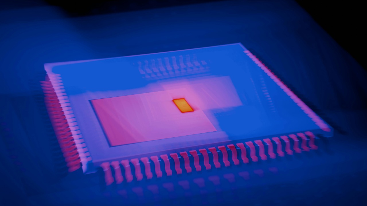
Inside the prototype: how the layers actually work
The team’s prototype is not a paper concept but a working chip that has already been put through early hardware tests. At its core is a set of logic layers that handle AI computation, topped and surrounded by dense memory layers that store weights and intermediate results directly above the circuits that use them. Vertical interconnects thread through these tiers, creating thousands of tiny, low-resistance pathways that let data hop between layers in a fraction of the time and energy required for a trip to off-chip DRAM. This is the architectural inversion that lets the device attack the memory wall head-on rather than trying to route around it.
Those early measurements are striking. The prototype already outperforms comparable 2D chips on key AI workloads, delivering higher throughput and lower energy per operation even before the design has been fully optimized. Reporting on The chip’s performance and potential notes that these gains come from the tight vertical integration of memory and logic rather than exotic new compute units, which suggests that further refinements in layout and process technology could push the advantage even further. In other words, the basic physics of shorter wires and denser locality are doing most of the work.
How the chip is actually manufactured
Building a monolithic 3D chip is far more challenging than stacking finished dies, because each layer must survive subsequent processing steps without being damaged. Until now, most attempts at 3D integration have relied on stacking separate chips that are fabricated independently, then aligned and bonded, a method that struggles to scale to many layers and often sacrifices yield. The new device instead uses a carefully tuned sequence of low-temperature steps so that additional transistor and memory layers can be grown on top of existing circuitry without melting or degrading what lies beneath.
Details from the project describe how the researchers refined this flow to keep the entire stack within the thermal budget of mainstream foundries, which is crucial if the technology is ever to move beyond the lab. A description of How the new 3D chip is made emphasizes that, until this work, monolithic 3D had largely been confined to small experimental structures rather than full AI accelerators. By demonstrating a complete stack that can be built with processes compatible with SkyWater Technology, the team is trying to position the approach as something that could eventually ride alongside, or even inside, the same fabs that manufacture the most advanced chips.
The people and institutions behind the breakthrough
Behind the technical diagrams are specific engineers who have been pushing monolithic 3D concepts for years. Two of the most visible figures are Indian-origin professors Subhasish Mitra and Tathagata Srimani, who are credited with building what is being described as America’s first monolithic 3D AI chip. Their work, highlighted under the banner “Meet Subhasish Mitra and Tathagata Srimani,” frames the device not just as a lab curiosity but as a milestone in US semiconductor research, with clear roots in the Indian academic diaspora.
The Stanford University research team has been central to this push, working with domestic manufacturing partners to translate academic ideas into silicon that can run real AI workloads. Reporting on The Stanford University research team notes that their monolithic 3D AI chip has already demonstrated up to 4× performance and energy gains compared with current two-dimensional benchmarks, a figure that has quickly become a rallying point for advocates of vertical integration. By pairing academic design expertise with a US foundry like SkyWater Technology, the group is also making a geopolitical statement about keeping cutting-edge AI hardware development onshore.
Measured gains: speed, energy, and real workloads
Performance claims in chip research are often theoretical, but in this case the numbers are grounded in hardware measurements. Early hardware tests show that the prototype already outperforms comparable 2D chips on AI inference tasks, with order-of-magnitude speed gains in some configurations. A report on US engineers develop 3D chip that offers order-of-magnitude speed gains underscores that these improvements come from integrating memory and computation vertically, which cuts the energy and time spent on data movement so sharply that the same workloads can be run faster or at much lower power.
Energy efficiency is just as important as raw speed, especially in data centers where electricity and cooling costs dominate. The Stanford University team’s monolithic 3D AI chip has been reported to hit roughly 4× gains in both performance and energy metrics compared with current two-dimensional benchmarks, meaning it can deliver the same throughput at a fraction of the power or significantly higher throughput within the same thermal envelope. Coverage of The chip’s performance and potential stresses that these results were obtained on a prototype that has not yet benefited from the full optimization and scaling that commercial products receive, which suggests that the ceiling for improvement is even higher.
How this compares with the HBM4 memory revolution
While monolithic 3D chips attack the memory wall by collapsing compute and storage into a single stack, the broader industry is also pushing hard on external memory bandwidth through high bandwidth memory. The shift to HBM4 in 2025 is being described as a watershed moment, with the new standard doubling the interface width to 2,048 bits and significantly increasing per-stack bandwidth. An analysis of The 2048-bit revolution argues that this wider interface is a gateway to unprecedented performance for GPUs and AI accelerators that can afford the cost and complexity of HBM4 stacks.
Yet even HBM4 is ultimately an external memory solution, with its own physical distance and power penalties. A companion piece on The Memory Wall: Why HBM4 is the New Frontier in the Global AI Arms Race describes the technical leap from HBM3e to a 2,048-bit interface and frames HBM4 as almost a processor in its own right, but it still relies on a high-speed link between logic and memory. Monolithic 3D chips, by contrast, aim to erase that boundary entirely by embedding memory directly above the compute units, which could complement HBM4 in high-end systems or offer a more integrated alternative in devices where board space and power are at a premium.
What this could mean for models like LLaMA and beyond
The practical test for any new AI chip is how it handles real models, not synthetic benchmarks. The research team has already used the prototype to run workloads based on Meta’s open-source LLaMA model, demonstrating that the architecture can support the kind of transformer networks that dominate today’s AI landscape. Reporting on Meta’s open-source LLaMA model notes that the chip’s vertical integration allows it to keep far more of the model’s parameters on-chip, reducing the need to stream data from external memory and smoothing out the performance cliffs that usually appear when models no longer fit in cache.
If such designs can be scaled to larger arrays, they could change the economics of both training and inference. For cloud providers, a 4× improvement in energy efficiency on transformer workloads translates directly into lower operating costs and the ability to serve more users per rack. For edge devices, from smartphones to autonomous vehicles, the ability to run complex models locally without massive power budgets could unlock new applications in real-time translation, perception, and decision-making. In that sense, the monolithic 3D chip is not just a faster engine, but a different way of organizing computation that could keep AI progress from stalling at the memory wall just as models are becoming most useful.
More from MorningOverview