Intel’s comeback in cutting edge manufacturing is no longer a vague roadmap, it now revolves around a single, spectacular machine: ASML’s latest High-Numerical Aperture Extreme Ultraviolet scanner. By installing the most advanced EUV tool on the planet and tying its future nodes to this platform, Intel is betting that access to ASML’s top equipment can reset the balance of power in the foundry race.
That bet is not just about bragging rights at sub-2 nanometers, it is about whether Intel can turn High-NA EUV into a durable lead over TSMC, Samsung and SK hynix in the Angstrom era, and convert that lead into real foundry business from hyperscalers and AI chip designers. The stakes run from the future of Intel Foundry to the trajectory of ASML’s own growth and the supply of the chips that will power large language models and other data hungry workloads.
High-NA EUV: the tool that defines the sub-2 nm race
The core of Intel’s new strategy is a specific class of lithography system that only one company can build. ASML, listed as AMS: ASML, has developed groundbreaking High-Numerical Aperture Extreme Ultraviolet tools that are explicitly designed to power the sub-2 nm era and reshape the semiconductor landscape for leading edge chip production, putting High NA EUV at the center of every advanced roadmap. These scanners are not incremental upgrades, they are the first tools engineered to keep Moore’s Law moving when conventional EUV and multi-patterning start to buckle under cost and complexity.
By design, High NA EUV increases the numerical aperture of the optics, which tightens the focus of the Extreme Ultraviolet light and allows smaller features to be printed with fewer exposures, a shift that directly improves yield and throughput at Angstrom scale nodes. ASML’s own positioning of these High NA systems as the platform for sub-2 nm logic means any foundry that wants to lead in that regime must secure capacity on these machines, and Intel’s decision to anchor its comeback on ASML’s top tier tools is a recognition that there is no alternative path to the front of the pack for leading edge chip production, as highlighted in ASML’s description of its High NA EUV tools.
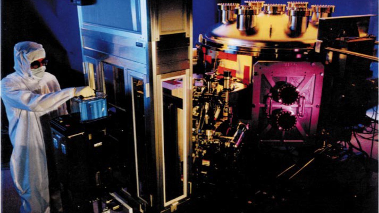
Intel’s first mover advantage with TWINSCAN EXE:5200B
Intel has turned that theory into hardware by becoming the first chipmaker to install ASML’s flagship High NA scanner. Intel Foundry announced that it has installed the world’s most advanced EUV machine, ASML’s TWINSCAN EXE:5200B, at its Oregon research and development facility, a milestone that shifts High NA from PowerPoint to powered on. The TWINSCAN EXE platform is the spear tip of ASML’s High NA line, and the EXE:5200B in particular is the configuration Intel is tying to its most ambitious node plans.
That installation is not a lab curiosity, it is explicitly tied to Intel’s 14A node, which the company has framed as the first process designed from the ground up around High NA EUV. Intel’s foundry arm has already completed successful acceptance testing of its first High NA EUV tool, a step that it describes as a major lithography milestone and a prerequisite for proving the economics of high volume manufacturing on this platform, underscoring how central the TWINSCAN EXE:5200B is to Intel’s 14A ambitions and its broader comeback narrative, as detailed in reports on Intel Foundry’s EXE:5200B install and the company’s first High NA EUV tool milestone.
The Angstrom era and Intel–ASML alignment
What makes this moment different from past node transitions is that Intel and ASML are moving in lockstep at the very front of commercialization. Reporting on the Angstrom era describes how Intel and ASML have solidified a lead in High EUV commercialization, positioning their partnership as the reference point for the first generation of Angstrom scale logic and the chips that will power large language models of the late 2020s. This alignment gives Intel early access to the most advanced configurations and process learning, while giving ASML a flagship customer that is willing to push the technology into production.
As of mid December, that collaboration is framed as the arrival of a new era in which High NA EUV is no longer a research project but a commercial tool that will underpin AI and other emerging technologies, with Intel and ASML explicitly named as the companies that have solidified the lead in High EUV commercialization. I see that as more than marketing language, it is a signal that both sides are prepared to invest heavily in ramping these tools, with Intel betting its foundry turnaround on them and ASML counting on that demand to drive its own growth, a dynamic captured in coverage of how Intel and ASML solidify their High NA EUV lead.
Capital, orders and the scale of Intel’s bet
Intel’s embrace of ASML’s top EUV tools is backed by an unusually large pool of outside capital, which underlines how expensive this comeback will be. In 2025, Intel received a USD 5 billion capital injection from NVIDIA and a USD 2 billion investment from SoftBank, funding that is explicitly linked to its foundry push and its need to secure more High NA EUV capacity from ASML. Those figures show that even rival chip designers and global investment groups see value in Intel’s access to leading edge manufacturing, provided it can secure enough of ASML’s scarce tools.
On the equipment side, Intel is ramping up orders for ASML’s new High EUV machines to prepare its 14A process against TSMC, with reports that it will receive another High NA EUV lithography machine from ASML soon as part of that ramp. The combination of USD 7 billion in fresh capital from NVIDIA and SoftBank and a growing queue of High NA EUV orders signals that Intel is not dabbling, it is committing to scale, a commitment that is spelled out in coverage of Intel’s USD 5 billion and USD 2 billion funding and its decision to increase ASML High NA EUV orders.
How High-NA EUV reshapes the competitive field
Intel’s early access to High NA EUV does not exist in a vacuum, it is already reshaping how rivals position themselves. Reporting on High NA adoption notes that Samsung is about a year behind Intel but ahead of TSMC and SK Hynix in adopting High NA EUV technology, a staggered timeline that gives Intel a window to prove out yields and costs before others bring their own High NA lines online. That sequence matters because the first company to demonstrate reliable Angstrom scale production with acceptable economics will have a powerful argument when courting AI and cloud customers.
At the same time, ASML’s own disclosures show that High EUV marks a milestone in commercialization, with ASML CEO Christophe Fouquet confirming during the company’s earnings call that the first High EUV tool has shipped and that this marks the start of large scale manufacturing. That means Intel’s lead is real but not unchallenged, since Samsung, TSMC and SK hynix are already in the queue for their own High NA EXE systems, including SK hynix receiving its first High EXE:5200 system, and the competitive gap will narrow as more of these tools move from Veldhoven to customer fabs, as described in reports on Samsung, Intel, TSMC and Hynix in High NA, ASML’s first High EUV commercialization milestone, and the first High EXE:5200 system at SK hynix.
Inside Intel’s 14A node and process roadmap
Intel’s 14A node is the first concrete test of whether High NA EUV can deliver a structural advantage over rivals. Intel has said that its upcoming 14A process node will use High EUV lithography and has framed that node as a historic release for the semiconductor industry, because it is the first to fully integrate High NA into a mainstream logic process. That choice is not just about shrinking features, it is about simplifying patterning, reducing the number of masks and exposures, and improving variability at Angstrom scale dimensions.
To support that, Intel announced that it had installed the industry’s first commercial High NA EUV lithography tool, the ASML TWINSCAN EXE:5200B, which it says sets the stage for 14A as feature dimensions continue to shrink and as it seeks to prove that High NA can be used in high volume manufacturing. Intel’s own press material reinforces that it is the industry’s first mover on High NA EUV lithography systems, and that Intel Foundry has received and is now qualifying these tools for AI and other emerging technologies, underscoring how tightly 14A, High NA and the comeback narrative are intertwined, as detailed in coverage of how TWINSCAN EXE:5200B sets the stage for 14A and Intel’s positioning as industry’s first mover on High NA EUV.
ASML’s growth ambitions and the High-NA revenue engine
For ASML, Intel’s aggressive adoption of High NA EUV is not just a technical validation, it is a revenue engine that underpins its own growth targets. ASML Holding has stated that it aims for about 30 percent year over year EUV revenue growth in its 2025 fiscal year, a goal that depends heavily on the ramp of both conventional and High EUV systems into logic and DRAM manufacturing. In DRAM manufacturing, these systems are already being used to support advanced nodes, and ASML is counting on a 23.8 percent year over year increase in overall revenue as part of this expansion.
That growth story is reinforced by the fact that ASML Holding stock is trading near its 52 week high, with investors responding to management’s confirmation that SK hynix received its first High EXE:5200 system and that this new wave of computing, driven by AI and large language models, will require exactly the kind of leading edge capacity that High NA EUV enables. From my perspective, Intel’s large orders and early installs are a central pillar of ASML’s confidence that it can hit those EUV revenue growth targets, as reflected in the company’s guidance on 30 percent EUV revenue growth and the market’s reaction to ASML Holding trading near a 52 week high.
Risks, execution challenges and the 18A pivot debate
No matter how advanced the tool, Intel still has to execute, and that is where the risks cluster. High NA EUV systems like the TWINSCAN EXE:5200B are among the most complex machines ever built, and reports on Intel’s install note that the company has had to work closely with ASML to stabilize the equipment and integrate it into its process flow, a reminder that first mover advantage also means first mover headaches. Intel’s own history of delays at 10 nm and 7 nm hangs over this effort, and the company cannot afford similar slips at 14A if it wants customers to trust its foundry roadmap.
There is also an active debate around Intel’s 18A technology and how it fits with the High NA pivot. Analysis of Intel’s strategy notes that the company is considering a pivot from 18A tech and that, moreover, Intel is widely recognized as the first chipmaker expected to deploy High EUV lithography at commercial scale, a status that could give the chip major a technological and strategic edge if it can align its node roadmap with the new tools. I see that as a sign that Intel is willing to adjust its plan to lean harder into High NA, but it also underscores that the company is still fine tuning how 18A, 14A and High EUV fit together, as captured in commentary on Intel’s pivot from 18A and High EUV edge.
Why Intel’s High-NA play matters beyond the fabs
The implications of Intel’s High NA EUV push extend far beyond its own fabs and ASML’s order book. As Intel jumps ahead with its next generation High NA EUV machine install, with reports highlighting how the company has moved first on the TWINSCAN EXE:5200B, it is effectively trying to reposition itself as the default Western alternative to TSMC for the most advanced AI and data center chips. That matters for cloud providers, automotive companies and governments that want geographic diversity in their supply of Angstrom scale silicon.
At the same time, ASML’s High NA EUV tools, described as reshaping the semiconductor landscape for leading edge chip production, are becoming a strategic asset in their own right, with access to these machines influencing where the most advanced AI accelerators, CPUs and memory are manufactured. If Intel can turn its early access into reliable 14A and beyond capacity, the combination of ASML’s High NA technology and Intel’s foundry ambitions could shift not just market share but also the geography of the Angstrom era, a shift foreshadowed in coverage of how Intel jumps ahead with High NA EUV and how ASML’s High NA tools reshape leading edge production.
More from MorningOverview