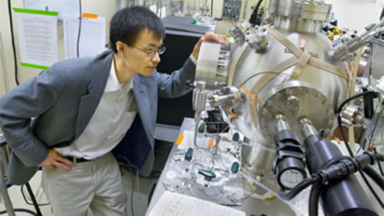
Researchers at the University of California, Berkeley, have pioneered a groundbreaking method to grow crystalline materials on-demand using visible light and liquid solutions. This innovative approach, led by Peidong Yang, allows for precise control over material formation in mere minutes, a significant leap from the traditional days-long processes. Detailed in a July 2023 study published in Nature, this advancement holds the potential to transform manufacturing in electronics and energy storage, offering customizable growth without the need for high temperatures or complex equipment.
The Breakthrough Method
The new technique leverages blue light to initiate the assembly of metal halide perovskite crystals from a precursor solution containing lead and halide ions. This process enables the formation of structures up to 100 micrometers in size within just 10 minutes. The key to this rapid crystallization lies in the use of photoacid generators, which release protons when exposed to light, thereby lowering the pH and triggering crystallization without the need for external catalysts. This method not only accelerates the growth process but also simplifies it significantly, as it operates under ambient conditions.
What sets this method apart is its on-demand capability, achieved through the projection of light patterns via a digital micromirror device. This allows for spatial control over where the materials grow, as they form only in the illuminated areas. Such precision opens up new possibilities for creating intricate designs and patterns in material manufacturing, paving the way for innovations in various technological fields.
Key Materials and Applications
The primary material grown using this method is methylammonium lead bromide (MAPbBr3) perovskites, known for their high-quality crystallinity, making them ideal for optoelectronic devices. This material’s superior properties could significantly enhance the performance of solar cells by enabling the efficient and scalable production of light-absorbing layers, potentially surpassing the current efficiency benchmarks of 25%. The ability to produce such materials quickly and efficiently could revolutionize the solar energy industry, making renewable energy more accessible and cost-effective.
Beyond solar cells, the method’s versatility extends to other materials, such as silver chloride crystals, which have applications in sensors and photocatalysis. This adaptability showcases the potential for broad applications across various industries, from environmental monitoring to advanced manufacturing processes, highlighting the method’s transformative impact on material science.
Advantages Over Traditional Techniques
Compared to conventional vapor deposition methods, which require temperatures above 400°C and vacuum chambers, this new approach operates at room temperature in aqueous solutions. This significant reduction in temperature and equipment complexity not only makes the process more accessible but also drastically cuts down on energy consumption. Crystals can form in under 5 minutes, a stark contrast to the 24 hours typically required for solution-based growth, reducing energy use by an impressive 90%.
The speed and cost benefits of this method are substantial, offering a more sustainable and economically viable alternative to traditional techniques. Peidong Yang emphasizes the scalability of this approach, stating, “This light-directed growth opens doors to additive manufacturing of functional materials.” Such advancements could lead to more efficient production lines and lower manufacturing costs, benefiting industries and consumers alike.
Challenges and Future Directions
Despite its promising potential, the method currently faces limitations, such as its restriction to small-scale patterns under 1 square centimeter. To fully realize its industrial applications, further optimization is necessary to scale up the process for larger volumes. Researchers at UC Berkeley’s Yang Lab are actively working on integrating this method with 3D printing technologies, aiming to create complex geometries suitable for biomedical implants and other advanced applications.
The broader implications for sustainable manufacturing are significant, as the solvent-based process minimizes waste compared to traditional solid-state synthesis. By reducing the environmental impact of material production, this method aligns with global efforts to promote sustainability in manufacturing. As research continues, the potential for this technology to revolutionize various industries remains vast, promising a future where materials can be grown quickly, efficiently, and with minimal environmental footprint.
More from MorningOverview